Unveiling the Magic: How Does a Printed Circuit Board Work? A PCB Deep Dive
What is a Printed Circuit Board (PCB)?
A Printed Circuit Board‚ or PCB‚ is the backbone of almost every electronic device you encounter daily. From your smartphone to your washing machine‚ PCBs provide the mechanical support and electrical connections for electronic components. They are essential for modern electronics. Without them‚ complex circuits would be impossible to miniaturize and mass-produce.
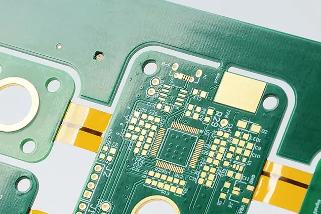
PCBs are typically made from a non-conductive substrate‚ such as fiberglass or composite epoxy‚ onto which conductive pathways‚ or traces‚ are etched. These traces connect various electronic components‚ allowing them to communicate and function together.
The Layers of a PCB
Understanding the layers of a PCB is crucial to grasping how does a printed circuit board work. PCBs can be single-layered‚ double-layered‚ or multi-layered‚ depending on the complexity of the circuit.
- Substrate: The base material‚ usually fiberglass‚ providing structural support.
- Copper Layer: Thin layers of copper foil etched to create conductive traces.
- Solder Mask: A protective layer that prevents solder bridges during assembly.
- Silkscreen: An ink layer used to print component designators and other information.
Multi-layered PCBs are particularly useful for complex circuits‚ as they allow for more intricate routing and signal management. Each layer can be dedicated to specific functions‚ such as power distribution or signal routing.
The Manufacturing Process
The manufacturing process of a PCB is a complex and precise undertaking. It involves several key steps‚ including:
- Design: Creating the circuit layout using CAD software.
- Printing: Transferring the design onto the copper layer.
- Etching: Removing unwanted copper to create the traces.
- Drilling: Creating holes for component leads and vias.
- Plating: Applying a thin layer of metal to the holes to create conductive vias.
- Solder Mask Application: Applying the solder mask to protect the traces.
- Silkscreen Printing: Printing component designators and other information.
- Testing: Ensuring the PCB meets the required specifications.
Each step requires careful control and precision to ensure the final PCB functions correctly. Automated equipment and rigorous quality control measures are essential for producing reliable PCBs.
How Components are Connected
Electronic components are connected to the PCB using various methods‚ including through-hole technology and surface-mount technology (SMT). Through-hole components have leads that are inserted through holes in the PCB and soldered on the opposite side. SMT components are soldered directly onto the surface of the PCB.
SMT is becoming increasingly popular due to its ability to accommodate smaller components and higher component densities. It also allows for automated assembly‚ which can significantly reduce manufacturing costs.
Interesting Fact: The density of components on a PCB can be incredibly high. Some advanced PCBs can have hundreds or even thousands of components per square inch!
Vias: The Vertical Highways
Vias are small holes drilled through the PCB that are plated with a conductive material. They are used to connect traces on different layers of the PCB. Vias are essential for multi-layered PCBs‚ as they allow signals to be routed between layers without having to run long traces on a single layer.
Frequently Asked Questions (FAQ)
Q: What are the common materials used for PCBs?
A: The most common materials are FR-4 (a fiberglass epoxy laminate)‚ but other materials like aluminum‚ Teflon‚ and flexible substrates are also used for specific applications.
Q: How can I design my own PCB?
A: You can use CAD software like Eagle‚ KiCad‚ or Altium Designer to create your PCB design. There are also many online resources and tutorials available to help you get started.
Q: What is the difference between single-sided and double-sided PCBs?
A: Single-sided PCBs have conductive traces on only one side of the board‚ while double-sided PCBs have traces on both sides. Double-sided PCBs are more versatile and can accommodate more complex circuits.
Q: What is impedance control in PCBs?
A: Impedance control is the process of designing PCB traces to have a specific impedance value. This is important for high-speed signals‚ as it helps to prevent signal reflections and ensure signal integrity.
Testing and Quality Assurance
Rigorous testing and quality assurance protocols are paramount in PCB manufacturing. These procedures ensure the reliability and functionality of the final product. Several testing methods are employed‚ including:
- Visual Inspection: A thorough examination for physical defects‚ such as scratches‚ voids‚ or misaligned components.
- Electrical Testing: Verifying the continuity and isolation of traces using specialized equipment. This includes continuity testing and insulation resistance testing.
- Functional Testing: Simulating real-world operating conditions to ensure the PCB performs as intended. This may involve loading the board with representative components and running specific test sequences.
- Automated Optical Inspection (AOI): Using cameras and image processing algorithms to detect defects that may be missed by visual inspection.
- X-Ray Inspection: Examining internal layers and solder joints for hidden defects‚ particularly in multi-layered PCBs and Ball Grid Array (BGA) components.
Failure to implement robust testing procedures can result in significant downstream issues‚ including product recalls‚ system failures‚ and reputational damage. Therefore‚ adherence to industry standards and best practices is crucial.
Advanced PCB Technologies
The field of PCB technology is constantly evolving‚ with new materials‚ manufacturing techniques‚ and design methodologies emerging regularly. Some advanced PCB technologies include:
- High-Density Interconnect (HDI) PCBs: Featuring finer lines and spaces‚ microvias‚ and buried vias to achieve higher component densities and improved electrical performance.
- Flexible PCBs: Constructed from flexible substrates‚ allowing them to be bent and shaped to fit into tight spaces or conform to complex geometries.
- Metal Core PCBs: Utilizing a metal core‚ typically aluminum or copper‚ to provide enhanced thermal dissipation capabilities. These are often used in high-power applications.
- RF and Microwave PCBs: Designed specifically for high-frequency applications‚ requiring careful consideration of impedance control‚ signal integrity‚ and material selection.
- 3D Printed PCBs: An emerging technology that allows for the creation of PCBs with complex geometries and embedded components.
These advanced technologies enable the development of increasingly sophisticated and compact electronic devices.
Design Considerations for Optimal Performance
Achieving optimal PCB performance requires careful consideration of several design factors. These include:
- Signal Integrity: Ensuring that signals are transmitted cleanly and reliably‚ without excessive noise or distortion. This involves careful routing of traces‚ impedance control‚ and the use of appropriate termination techniques.
- Power Distribution: Providing a stable and reliable power supply to all components on the PCB. This requires careful planning of power planes‚ decoupling capacitors‚ and trace widths.
- Thermal Management: Dissipating heat effectively to prevent overheating and component failure. This may involve the use of heat sinks‚ thermal vias‚ and careful component placement.
- Electromagnetic Compatibility (EMC): Minimizing the emission of electromagnetic interference (EMI) and ensuring that the PCB is immune to external EMI. This requires careful shielding‚ grounding‚ and filtering techniques.
- Manufacturability: Designing the PCB in a way that is easy to manufacture and assemble. This involves adhering to design rules‚ minimizing the number of layers‚ and selecting components that are readily available.
A holistic approach to PCB design‚ considering all of these factors‚ is essential for creating reliable and high-performing electronic devices.
Important Note: Grounding is crucial for signal integrity and EMC performance. A well-designed ground plane can significantly reduce noise and improve overall system performance.